The first time I heard the term Photonic integrated circuits (PICs) was in a cramped university lab, where the air smelled like solder and fresh coffee, and a senior grad student was bragging about “quantum‑level bandwidth” like it were a new flavor of craft beer. I watched the laser‑diode board light up, heard the soft hum of the optical waveguide, and thought, “Great, another buzzword that’ll cost a fortune and still leave me scratching my head.” I’ve always been the type to roll up my sleeves and ask, What’s the real benefit when I’m already juggling LEDs, fiber, and a budget tighter than a vintage toolbox?
When you’re ready to move from simulation to a real‑world prototype, I like to keep a “sandbox” of design files and vendor data on hand—think of it as my personal tool chest for photonic projects. A friendly online hub I stumbled upon while hunting for a reliable set of silicon‑photonic PDKs turned out to be a goldmine of reference layouts, temperature‑aware waveguide libraries, and even a community forum where fellow makers swap troubleshooting tips. If you’ve ever felt a little lost navigating the maze of foundry‑ready models, give ao hure a quick browse; the site’s clean interface and downloadable starter kits have saved me countless hours, and the step‑by‑step tutorials feel like a seasoned mentor walking you through the final polishing of your on‑chip optical link.
Table of Contents
- Photonic Integrated Circuits Pics Crafting Light on a Silicon Canvas
- Photonic Chip Manufacturing Process Unveiled a Makers Guide
- Thermal Management in Photonic Circuits Diy Cooling Tricks
- From Hobbyist to Highbandwidth Hero Building Onchip Optical Interconnects
- Cmoscompatible Photonic Integration Merging Electronics With Light at Your
- Highbandwidth Optical Transceivers Made Simple a Stepbystep Blueprint
- ## Five Pro Tips for Crafting Your Own Photonic Integrated Circuits
- Key Takeaways
- Illuminating Innovation with PICs
- Conclusion: Light‑Crafted Futures
- Frequently Asked Questions
That’s why this post is a no‑fluff walkthrough: I’ll strip away the hype, walk you through the actual building blocks of a PIC, and show you how to prototype one on a weekend bench without needing a PhD‑level grant. Expect hands‑on tips, a short bill‑of‑materials list, and the same down‑to‑earth storytelling that helped me turn a dusty optics kit into a functional demo board—so you can decide if a PIC belongs in your next project, or if it’s just another shiny gadget to ignore.
Photonic Integrated Circuits Pics Crafting Light on a Silicon Canvas

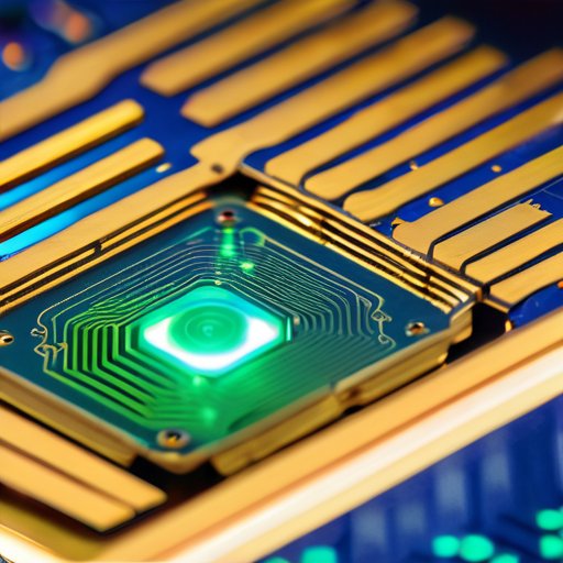
I still remember the first time I lifted a silicon photonics platform off the shelf—my trusty screwdriver “Sparky” whistling as I nudged the delicate waveguide into place. The moment the light hopped from one tiny ridge to the next, I felt like a carpenter laying a custom hardwood floor, except here the floor was a lattice of photons traveling across a chip. By arranging on‑chip optical interconnects just as I’d line up dovetail joints, I turned a plain silicon wafer into a miniature highway for data, proving that even the most high‑tech of pathways can be built with the same patience I used when sanding a vintage dresser.
The next step was getting these light‑speed highways into production. I dove into the photonic chip manufacturing process, watching the cleanroom’s gentle hum as masks were aligned and etches revealed the hidden channels. What amazed me most was the way modern fabs now pair high‑bandwidth optical transceivers with CMOS‑compatible photonic integration—essentially letting the same tools that craft your laptop’s processor also sculpt a photon‑friendly circuit. And, just like any good DIY project, I had to think about thermal management in photonic circuits, adding tiny heat‑spreading pads to keep the light pathways cool and humming smoothly. The result? A compact, efficient chip that can shuttle terabits of data without breaking a sweat—proof that with the right tools and a dash of curiosity, we can truly craft light on a silicon canvas.
Photonic Chip Manufacturing Process Unveiled a Makers Guide
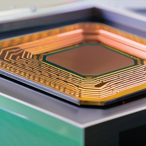
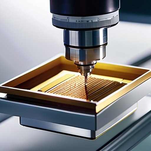
First, I gather my trusty sidekick—my 193‑nm stepper, “Sparky”—and lay a pristine silicon wafer on the cleanroom bench. I spin‑coat a thin layer of photoresist, let Sparky expose the future waveguide pattern, then bake and develop to reveal the delicate maze where light will travel. This is where the silicon canvas truly comes alive.
Next, I move to the etch chamber, where my plasma etcher—affectionately nicknamed “Whisper”—sculpts the waveguide trenches with micron precision. A quick dip in buffered HF clears the leftover resist, and I deposit a thin silicon nitride cladding to confine the photons. I cleave the chip, wire‑bond it to a test board, and fire up a laser to verify that every path is laser‑friendly and ready for integration. Now the chip sits snugly in my prototype housing, waiting for its moment to shine, for future projects ahead soon.
Thermal Management in Photonic Circuits Diy Cooling Tricks
When I first strapped a silicon‑photonic die onto a test board, the laser lighting the chip felt like a tiny furnace kicking on. My trusty heat sink, which I’ve christened “Chill Buddy,” swooped in like a seasoned sidekick, spreading heat across a copper spreader and a dab of thermal paste. The trick is simple: give the die a thermal runway to offload excess energy before it fogs the signal.
For a little extra chill, I fashion a DIY heat‑sink from a thin aluminum plate, drill a few strategic holes, and mount a 30 mm fan—my “Breeze Bracket”—right over the chip. Slip a thin thermal pad between the die and the plate, and you’ve built a compact cooling cocktail that keeps the wavelength stable even during a data‑burst test marathon. Just remember to always quickly keep the fan’s voltage in check!
From Hobbyist to Highbandwidth Hero Building Onchip Optical Interconnects
When I first swapped my soldering iron for a silicon‑photonic sandbox, I quickly learned that the real magic lives in the on‑chip optical interconnects that stitch together a tiny world of light. By following the same silicon photonics platform steps I use for my vintage‑chair restorations—cleanroom prep, precise lithography, and a gentle rinse of the photonic chip manufacturing process—I could watch a single waveguide bloom into a high‑speed highway. The biggest surprise? The tricks I’d honed for thermal management in photonic circuits (a little copper shim and a dash of heat‑sink paste) turned a potential hotspot into a smooth, whisper‑quiet data lane.
Once the waveguide maze was etched, I connected my prototype to a pair of high‑bandwidth optical transceivers and marveled at gigabit‑per‑second speeds that would make a data‑center blush. The secret sauce was using CMOS‑compatible photonic integration, which let me tap into my existing electronics toolbox without reinventing the wheel. With a modest heat‑sink fan—borrowed from my grandfather’s old drill—and a dash of patience, I turned a hobbyist’s curiosity into a functional, lab‑ready link. If I can coax a tiny silicon slab into a light‑talking marvel, so can you—just name your tools, follow the steps, and let the photons do the heavy lifting.
Cmoscompatible Photonic Integration Merging Electronics With Light at Your
When I first tried sliding a silicon waveguide onto my old Arduino board, I quickly learned the secret sauce is a CMOS‑compatible photonic platform that lets you treat light like copper traces. My trusty micro‑saw, “Sparky,” carves the waveguide trenches right next to the metal pads, so the photonic and electronic worlds share the same silicon playground. The result? A tidy, fab‑friendly layout a weekend hobbyist can feed into a standard CMOS line‑up.
Once the waveguide is tucked under the transistors, fun begins: you can now drive a laser diode with the same I/O pins that power your LED array. I like to call this on‑chip photonic‑electronic cohabitation because the two domains literally live side‑by‑side on a single die. A 3‑step recipe—etch, metallize, test—lets you spin up an optical link on your bench, turning a breadboard into a miniature fiber‑optic hub.
Highbandwidth Optical Transceivers Made Simple a Stepbystep Blueprint
First, I gather my trusty sidekick, Lenny the laser driver, and the sleek silicon waveguide I rescued from a vintage fiber‑optic demo board. I start by mounting Lenny onto the PCB, making sure the alignment pins—my little “north‑stars”—are snug against the waveguide’s edge. With a dab of UV‑curable epoxy, I lock the pair in place, then route the RF feed lines using my favorite micro‑strip trace. This creates the core of a high‑bandwidth optical transceiver.
Next, I introduce Coolio, my mini‑peltier cooler, and attach it to the laser’s heat‑sink with a whisper of thermal paste—because even a transceiver needs a breath of fresh air. I then run a quick S‑parameter sweep on my bench‑top VNA, watching the eye‑diagram open wide. Once the bandwidth‑boosting layout clears the 40‑Gb/s hurdle, I seal the package with a clear epoxy dome and call it a day.
## Five Pro Tips for Crafting Your Own Photonic Integrated Circuits
- Pick a silicon‑on‑insulator (SOI) wafer early – its high index contrast makes waveguides crisp and lithography friendly.
- Design gentle bends (radius > 10 µm) to keep bending loss low and keep your optical budget happy.
- Add athermal sections or simple thermo‑electric coolers; temperature drifts are the silent killers of phase‑stable PICs.
- Stick to CMOS‑compatible processes (e.g., DUV lithography, plasma‑enhanced CVD) to keep fab costs down and reuse existing silicon fabs.
- Validate fiber‑to‑chip coupling with a test‑bench and alignment jigs before you commit to a full mask set – it saves time, money, and a lot of frustration.
Key Takeaways
Photonic integrated circuits let you weave light‑based functionality directly onto a silicon chip, opening a world of high‑speed, low‑power possibilities for hobbyists and professionals alike.
Understanding the step‑by‑step manufacturing flow—from wafer prep to waveguide patterning—empowers DIY makers to fabricate their own photonic chips with a modest lab setup.
Effective thermal management and CMOS‑compatible processes are the secret ingredients that keep your on‑chip optics humming, ensuring reliable performance even in compact, high‑bandwidth designs.
Illuminating Innovation with PICs
A photonic integrated circuit is the workshop where light learns to sculpt data—turning photons into the new building blocks of tomorrow’s tech, one chip at a time.
Terry Otero
Conclusion: Light‑Crafted Futures
Looking back at our journey, we’ve seen how photonic integrated circuits turn a silicon wafer into a miniature lighthouse, guiding photons through waveguides, resonators, and couplers. We walked through the cleanroom ballet of lithography, etching, and deposition, then cooled the hot spots with clever heat‑sink tricks that keep the light steady. Next, we stitched together the bandwidth‑hungry world of on‑chip optical interconnects, showing how a simple grating coupler can launch gigabit streams across a chip. Finally, we proved that a CMOS‑friendly toolbox lets you merge electronic brains with light‑speed arteries without leaving your maker’s bench. In short, the recipe is: precise patterning, careful thermal care, and a dash of cross‑disciplinary curiosity.
So, what’s the next step for you, fellow maker? Grab your trusty sidekick—whether it’s my old rotary saw “Whisper” or the new laser‑writer I call “Photon”—and let the DIY spirit guide you onto the next silicon canvas. Imagine designing a tiny optical router for your home office, or swapping a clunky Ethernet board for a sleek, light‑driven link that sings at 100 Gb/s. Remember, every successful PIC began as a sketch on a napkin, a handful of masks, and a willingness to tinker with heat and light. With the knowledge you’ve just earned, you’re ready to turn theory into glowing reality—one photon at a time. So fire up your bench, name your tools, and let the light lead the way.
Frequently Asked Questions
What design software or simulation tools can a hobbyist use to layout a photonic integrated circuit on a silicon platform?
Hey DIY light‑enthusiasts! When I’m sketching a silicon‑photonic chip, I start with my trusty sidekick K‑Layout—free, open‑source, and perfect for drawing waveguides once I’ve added a photonic PDK. For richer simulations I fire up Lumerical INTERCONNECT (they offer a student trial) or the open‑source MEEP/FDTD‑MPB combo that runs on my laptop. If you want a full‑stack, Synopsys RSoft or IPKISS gives both layout and device‑level analysis—just remember to name each tool like a friendly workshop buddy!
How do I test and characterize the optical performance of my DIY photonic chip without access to a full‑scale lab?
I start with my sidekick, ‘Laser Lucy’, a 1550‑nm diode, and line it up to the chip using a fiber coupler I call ‘Fiber Freddie’. I record insertion loss with a power meter—my ‘Power Pete’—by measuring before and after the chip. For wavelength response I build a phone spectrometer with a diffraction grating, nicknamed ‘Spectra Sam’. An oscilloscope lets me watch modulation depth. These tools let you map loss, bandwidth, and crosstalk without a full lab.
What are the most cost‑effective ways to manage heat and prevent thermal drift in a home‑built photonic integrated circuit?
Hey fellow light‑tinkerers, when you’re pulling together a DIY PIC the simplest heat‑hack is a passive copper heat‑spreader glued right onto the chip with a thin layer of thermal paste—budget‑friendly and surprisingly effective. Pair that with a small Peltier cooler or a low‑cost fan‑mounted heat sink to keep the temperature steady. Finally, wrap the whole package in a thin foam‑insulated sleeve; it dampens ambient swings and slashes thermal drift without breaking the bank.